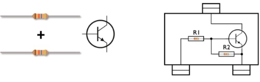
To reduce the number of components and simplify circuit board design, a resistance transistor combines one or two bipolar transistors with a bias resistor and integrates them on the same chip. Alternatives include paralleling a second integrated resistor along the base-emitter path to create a divider for setting the base voltage. This can provide finer tuning and better turn-off characteristics. Because the tolerance of these internal resistors is higher than that of the external resistors, RET is suitable for switching applications where transistors operate in the on or off state. For this reason RET is sometimes referred to as a digital transistor. This paper discusses some key operating parameters when designing with RET in switching applications.
Resistor transistor (RET)
Voltage and current (VI) parameters
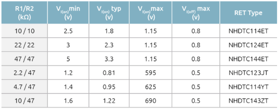
IC/IIN refers to the current gain hFE of RET, where IIN includes the base current and the current flowing through R2 (IR2 = VBE/R2). Thus, hFE is smaller than RET, which has only one series base resistor, R1. Because the input current is shunt from the base, the lower the R2 value, the lower the hFE value. This can be seen in Table 1. VCEsat is the residual collector-emitter voltage of RET switch when it is on.
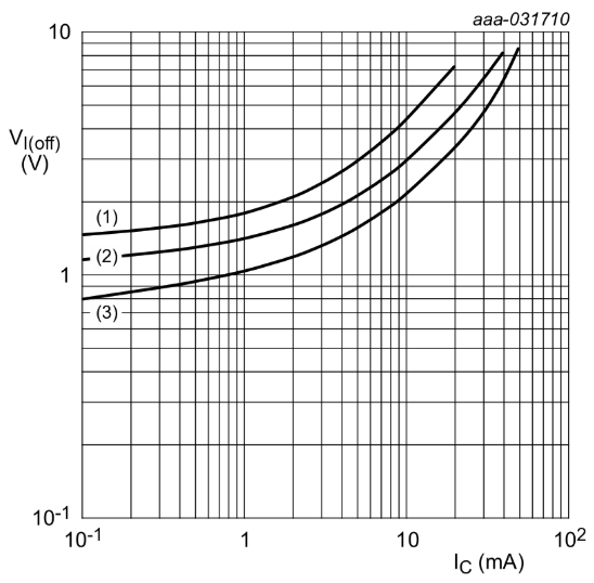
The test condition for measuring hFE is to apply a base current of 0.5 mA and a collector current of 10 mA. Vi(off) is the input voltage when the RET device is turned off. In this case, the collector leakage current is 100µA and the collector-emitter voltage (VCE) is 5 V. The lower V(Ioff)max value provided in the table is the maximum allowable output level for the RET driver stage. This condition must be met to ensure the safe operation of RET in the off state. VI(on)min is the most critical parameter when testing RET in the on-off state. The circuit used to drive the RET must be able to provide this voltage level to ensure safe opening. The on-state refers to the state where the collector current is 10 mA when the collector-emitter voltage is 0.3 V. The VI rating specified in the RET data manual is valid for these test conditions only. RET requires a larger base drive voltage VI(on) to obtain a larger switching current. Figure 2 shows the voltage-current (VI) switching characteristics of RET transistors.
● VI < VI(off)max: All RET devices are guaranteed to be turned off
● Vi < Vi(off)typ: The typical RET is off
● Vi < Vi(off)typ: The typical RET is in the on-off state
● VI > VI(on)min: All RET devices are guaranteed to be on
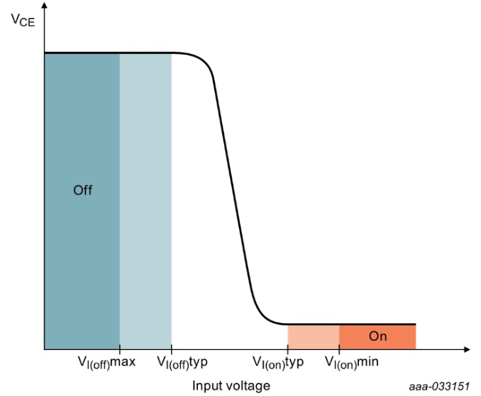
Table 1 shows the dependence of the input voltage in the on and off states on the resistive voltage divider configuration in the Nexperia NHDTC series RET. At VI(off), a tiny base current will flow through the transistor (about 0.3 µA). The typical value of the voltage required to turn off RET is related to the resistance ratio R1/R2. When the transistor is off, this value can be calculated using R2 or the voltage drop target at either end of the base-emitter diode. For the NHDTC series, the voltage is about 580 mV. Thus, the VI(off) value at a resistance ratio of 1 has the same voltage (lines 1-3 in Table 1). For this reason, the typical voltage value of the off state is lower when R2 is 47 kΩ and R1 is 2.2 kΩ, 4.7 kΩ, or 10 kΩ. VI(off) max needs to be even to ensure that the device operates in the dark green shaded area on the far left in Figure 2.
Nexperia's RET portfolio
The correct selection of the resistance divider is essential to ensure that the control voltage range of the RET matches the driver stage. The required collector or load current affects the base current provided for the on-on state. A higher collector current can be set using a lower R1 and/or a smaller bypass current flowing through R2.
In addition to the universal series, Nexperia (Anse Semiconductor) offers RET devices with enhanced features, for example, the NHDTA/NHDTC series RET(see Table 1) has a VCEO of 80 V. This feature makes these devices ideal for 48 V automotive applications. The PDTB and PBRN series RETs support 500/600 mA collector currents and can be used in switching power relays and power leds.
Notes on temperature
In practical applications, pay close attention to the temperature drift of VI parameter. The VBE of BJT decreases with increasing temperature, with coefficients ranging from -1.7mV/K to -2.1mV/K. As shown in Figure 3, hFE will also increase by about 1% per Kelvin for independent BJTS.
The typical DC current gain is a function of the collector current

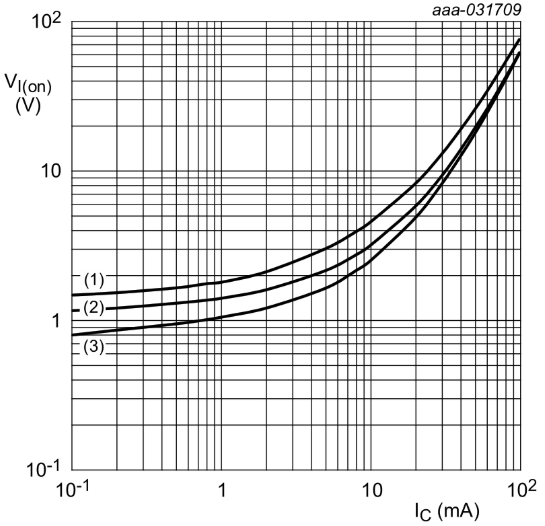
VI(on) is a function of IC, so higher input voltage is required to drive more collector current at the same VCE. Low ambient temperatures require higher input voltages because hFE decreases as VBE increases. The RET switch therefore needs to be turned on at low temperatures, which is a critical operating condition for the application, and sufficient input voltage is required to turn the device on correctly (Figure 4).
The input voltage in typical on-state is a function of collector current
In the off - off state, high temperature conditions are critical. Therefore, the drive circuit must be designed to have an output voltage well below VI(off) typical at the highest application temperature (Figure 5).
The input voltage in typical on-state is a function of collector current
Simple, but safe and reliable
RET is a relatively simple device that is well suited to switching applications. Nevertheless, designers must be aware of the parameters that affect its operation, including switching voltage and current, and how it is affected by temperature. This blog post provides design tips to ensure that Nexperia's RET works safely and reliably in targeted applications.
| Référence | Description | |
|---|---|---|
| RETENTIONCLIP(2X) Bel Power Solutions |
Accessoires, MATING CONN CASSETTE STYLE | RFQ |
Traction inverters are the main battery drain components in electric vehicles (EVs), with power levels up to 150kW or higher. The efficiency and performance of traction inverter directly affect the driving range of electric vehicle after a single charge. Therefore, in order to build the next generation of traction inverter systems, silicon carbide (SiC) field effect transistor (FET) is widely used in the industry to achieve higher reliability, efficiency and power density.
Do you know the 8 application circuits of operational amplifiers?
This technical presentation requires an understanding of how to configure an operational amplifier in a typical gain control circuit. The applications of linear and nonlinear digital potentiometers are discussed. This article gives an overview of the basic techniques required to convert audio and other potentiometer/op amp applications from conventional mechanical potentiometers to solid state potentiometers
The current in an electronic circuit usually has to be limited. In USB ports, for example, excessive current must be prevented to provide reliable protection for the circuit. Also in the power bank, the battery must be prevented from discharging. Too high discharge current results in too large voltage drop of the battery and insufficient supply voltage of downstream devices
Using advanced real-time control technologies such as motor control circuits with higher power density, higher integration and more efficient systems, better acoustic performance of the system can be achieved
Brushless direct current (BLDC) motors have been widely used in household appliances, industrial equipment and automobiles. While brushless DC motors offer a more reliable and maintainable alternative to traditional brushless motors, they require more sophisticated electronics to drive them
How to achieve precise motion control in industrial actuators
The NCP51820 is a 650 V, high-speed, half-bridge driver capable of driving gallium nitride (" GaN ") power switches at dV/dt rates up to 200 V/ns. The full performance advantages of high voltage, high frequency and fast dV/dt edge rate switches can only be realized if the printed circuit board (PCB) can be properly designed to support this power switch. This paper will briefly introduce NCP51820 and the key points of PCB design of high performance GaN half bridge grid driver circuit using NCP51820