The NCP51820 is a fully functional dedicated driver designed to take full advantage of the switching performance of a high electron mobility transistor (HEMT) GaNFET. Compared to silicon devices with similar breakdown voltage ratings, the chip size used to manufacture GaNFET is smaller. As a result, the gate charge, output capacitance, and dynamic on-resistance of GanFets are greatly reduced, even compared to the best silicon MosFeTs in their class. In addition, the GaNFET has no PN junction, so there is no intrinsic parasitic diode on the drain-source pole and no reverse recovery charge associated with the third quadrant operation.
GaNFET is ideal for off-line half-bridge power topologies, bridless PFCS, and single-ended active clamped topologies. These power levels often use zero voltage switches (ZVS), but can also operate at around 400V in hard switching conditions. All of these improvements allow GaNFET to switch at or near frequencies in the MHz range, with drain-source edge rates up to 100V/ns. Achieving optimal performance for GAN-based power levels depends to a large extent on the designer's understanding of parasitic circuit components (such as package inductors, PCB routing inductors, transformer capacitors) and component selection and layout. Although these parasitic elements are also present in silicon MOSFET power systems, in GaN power solutions, there is a more pronounced response when subjected to the high dV/dt and di/dt excitation present therein, and therefore a problem.
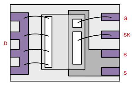
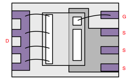
The NCP51820 MLP leadless power package (FIG. 3) and various leadless GaNFET power packages in the industry (FIG. 1 and FIG. 2) demonstrate design efforts to sufficiently reduce parasitic inductance. Similarly, particular attention must be paid to PCB design and component layout. In order to take full advantage of GaN power switches used in the NCP51820 drive high-speed half-bridge power topology, there are some important PCB design factors to consider, and this white paper will focus on some of these important considerations.
Package description for HEMT GaN and NCP51820
Most GaNFET packages contain a dedicated source Kelvin return pin, as shown by the "SK" in Figure 1, which serves only to send the gate drive return current back to the NCP51820. Higher current leak-source pins are welded to multiple pads through multiple welding wires, but for brevity, the simplified diagram in Figure 1 shows only one welding wire connection. The interface between the NCP51820 output and the GaNFET grid source Kelvin pins must be a direct single point connection. This interface is particularly important, as described in the GaNFET section containing the source Kelvin pins.
However, not all GanfeTs include a dedicated source Kelvin return pin, such as the example shown in Figure 2. For GanFets that do not contain source Kelvin return pins, special care must be taken when wiring the grid drive portion of the PCB design. For the switch node connection of the half-bridge power level, the source pole of the GaNFET on the high voltage side is directly connected to the drain pole of the GaNFET on the low voltage side to form a high dV/dt node with high di/dt load current. Direct use of the gate drive return pin of this high voltage switch node is not recommended, as described in the GaNFET section without the source Kelvin pin.

Figure 1. A typical GaN with source Kelvin return pins

Figure 2. A typical GaN without the source Kelvin return pin
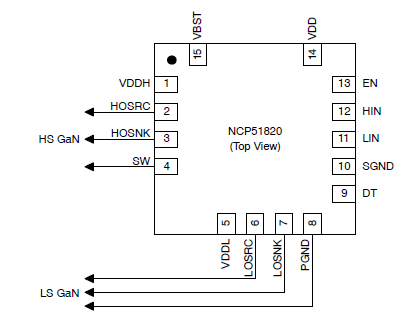
The NCP51820 comes in a 4x4 mm leadless package, with all logic level input and programming functions set to the right of the IC, separate from the power functions strategically located on the remaining three sides of the IC. Pin placement based on design strategy to provide high voltage isolation if necessary. The following PCB layout section explains the advantages of pin allocation in the NCP51820.

Figure 3. Pin allocation for NCP51820 GaN driver
Summary of PCB design strategy
When starting a PCB design using GaNFET, it is best to consider the entire layout according to priority, as listed below.
1) A multilayer PCB design must be used and the ground/return plane shall be used appropriately as described in this article. High frequency, high voltage, high dV/dt and high di/dt require multi-layer PCB design. To achieve the full benefits of GaN based power levels, the ground plane must be properly wired or designed in a way that inexpensive single layer PCB designs cannot.
2) At the beginning, the most noise-sensitive components should be placed near NCP51820. VDD, VDDH and VDDL bypass capacitors and VBST capacitors, resistors and diodes should be as close to their respective pins as possible.
3) Place the DT resistor directly between DT and SGND pins.
4) HO and LO, pull current and fill current grid drive resistors should be as close to GaNFET as possible.
5) Move NCP51820 and associated components as close as possible to GaNFET pull current and fill current resistance.
6) If possible, arrange the GaNFET so that HO and LO grid drive lengths match as closely as possible. In order to avoid high current and high dV/dt flows through the hole, the two ganFets should preferably be located on the same side of the PCB as the NCP51820.
7) HO and LO grid drives should be considered as two separate, electrically isolated grid drive circuits. Therefore, HO and LO each require dedicated copper contact (copper land) return planes on Layer 2, directly below the grid drive wiring on Layer 1.
The correct wiring of power loop, switch node, grid drive loop and using plane are very important for GaN PCB design. If there is a need for this part of content, a new article with illustrations may be sent later to explain each item. For gate drivers, proper wiring and noise isolation will help reduce additional parasitic loop inductance, noise injection, ringing, gate oscillation, and accidental on-off. The objective is to design a high frequency power PCB with careful consideration of proper grounding while allowing controlled current to flow through the direct path connection with minimal loop distance.
Component layout and wiring
Figure 4 highlights the key component layout around the NCP51820 and the interface to HS and LS GaNFET.

Figure 4. NCP51820 component layout
A GaNFET containing source Kelvin pins
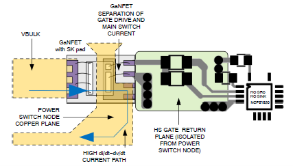
Many GaNFET packages include a dedicated source Kelvin pin that isolates the gate drive return current from the higher current and voltage levels that occur at the power switch node (high voltage side) or at the power supply ground (low voltage side). For GanfeTs with dedicated source Kelvin pins, grid driver wiring is fairly simple. The recommended PCB routing design example is shown in FIG. 5. It can be seen that the return current of GaNFET grid driver on the high voltage side is effectively separated from the current of the power switch node.

Figure 5. Source Kelvin GaNFET wiring
GaNFET without source Kelvin pin
Some GaNFET packages do not include dedicated source Kelvin pins, and careful consideration must also be given to isolating the gate drive return current from the higher current and voltage levels that occur at the power switch node (high voltage side) or at the power supply point (low voltage side). For GanFets without dedicated source Kelvin pins, an additional length of copper etched wire should be connected from the GaNFET source whose sole function is to send the gate drive return current back to NCP51820.
Although not as efficient as dedicated Kelvin pin connections, this wiring technique can still achieve an acceptable degree of separation between grid drive current and power switch nodes. The recommended PCB routing design example is shown in Figure 6. It can be seen that the return current of GaNFET grid driver on the high voltage side is effectively separated from the current of the power switch node. Regardless of the type of GaNFET package, the design goal is to avoid exposure of the NCP51820 and supporting circuits to potentially destructive switching voltages and currents flowing through the power level.

Figure 6. GaNFET wiring with passive Kelvin pin
| Référence | Description | |
|---|---|---|
| NCP5183DR2G ON Semiconductor |
Durée de conservation, IC DRIVER HI/LO 600V 8SOIC | RFQ |
| NCP5181PG ON Semiconductor |
Durée de conservation, IC MOSFET DVR HIGH VOLT 8-DIP | RFQ |
| NCP5181DR2G ON Semiconductor |
Durée de conservation, IC MOSFET DRVR HIGH VOLT 8-SOIC | RFQ |
Traction inverters are the main battery drain components in electric vehicles (EVs), with power levels up to 150kW or higher. The efficiency and performance of traction inverter directly affect the driving range of electric vehicle after a single charge. Therefore, in order to build the next generation of traction inverter systems, silicon carbide (SiC) field effect transistor (FET) is widely used in the industry to achieve higher reliability, efficiency and power density.
Do you know the 8 application circuits of operational amplifiers?
This technical presentation requires an understanding of how to configure an operational amplifier in a typical gain control circuit. The applications of linear and nonlinear digital potentiometers are discussed. This article gives an overview of the basic techniques required to convert audio and other potentiometer/op amp applications from conventional mechanical potentiometers to solid state potentiometers
The current in an electronic circuit usually has to be limited. In USB ports, for example, excessive current must be prevented to provide reliable protection for the circuit. Also in the power bank, the battery must be prevented from discharging. Too high discharge current results in too large voltage drop of the battery and insufficient supply voltage of downstream devices
Using advanced real-time control technologies such as motor control circuits with higher power density, higher integration and more efficient systems, better acoustic performance of the system can be achieved
Brushless direct current (BLDC) motors have been widely used in household appliances, industrial equipment and automobiles. While brushless DC motors offer a more reliable and maintainable alternative to traditional brushless motors, they require more sophisticated electronics to drive them
How to achieve precise motion control in industrial actuators
The NCP51820 is a 650 V, high-speed, half-bridge driver capable of driving gallium nitride (" GaN ") power switches at dV/dt rates up to 200 V/ns. The full performance advantages of high voltage, high frequency and fast dV/dt edge rate switches can only be realized if the printed circuit board (PCB) can be properly designed to support this power switch. This paper will briefly introduce NCP51820 and the key points of PCB design of high performance GaN half bridge grid driver circuit using NCP51820