We live in an age of being wrapped in electronic devices that make learning, working, exercising, traveling and communicating very convenient, and wearables in particular are becoming an integral part of People's Daily lives. In medical applications, wearables can be used to monitor heart rate, blood pressure, blood oxygen levels, calories burned during exercise, sleep tracking and more. To provide a better user experience, high performance, small size and low power consumption are key metrics for these wearables. Of course, achieving all of these goals often requires trade-offs in circuit design, such as increasing the size of the device to meet specific power consumption goals. So is there a way to effectively extend battery life without increasing the size of these battery-powered devices?
The answer, of course, is yes. First of all, the development trend of miniaturization, low power consumption and high performance of electronic components is very conducive to the small size design requirements of wearable devices. Second, fast charging and advanced power management IC (PMIC) technologies are widely used in wearable devices. In recent years, with the gradual improvement of SIMO PMIC technology, the power design of wearable devices has become easier.
Power management in wearable devices
According to analysis by Mordor Intelligence, the wearable technology market is estimated to be worth approximately $27.91 billion in 2020 and is expected to reach $74.03 billion by 2026, with a compound annual growth rate (CAGR) of 17.65% over the forecast period (2021 to 2026). Especially the appearance of MEMS sensor has further accelerated the development of wearable technology. For example, by integrating these sensors into a dedicated wearable device, people could monitor their physical fitness from anywhere, anytime, using a wearable fitness tracking system. The number of connected wearable devices globally is expected to grow from 593 million in 2018 to 1.105 billion in 2022, according to Cisco.
The market forecast data from Grand view Research is even more optimistic, with their analysts believing that the global wearable technology market reached $40.65 billion in 2020 and is expected to grow at a compound annual growth rate (CAGR) of 13.8% from 2021 to 2028.
The main factors contributing to the rapid development of the market come from two aspects:
● One is that advances in technology such as the Internet of Things (IoT) have led to a proliferation of connected devices that are rapidly growing in popularity;
● Second, rising rates of chronic disease and obesity have prompted the adoption of wearable products, such as activity trackers and body monitors, to monitor users' overall health and provide real-time data.
These wearables also provide information related to daily events and physiological data, such as sleep quality, heart rate, blood oxygen levels, blood pressure, cholesterol levels and calories burned.
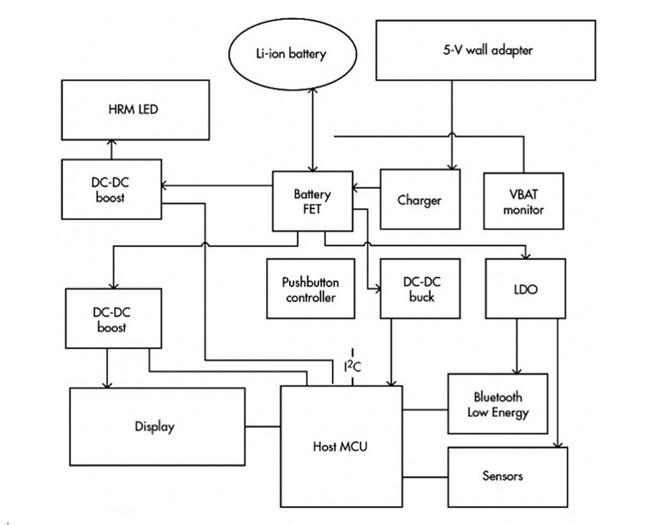
Wearable devices usually consist of modules such as microcontrollers, memory, communications, displays, sensors and power management. Microcontrollers, displays, and sensors may have different voltage requirements. Many peripherals such as communication ics and sensors spend most of their time in sleep mode and power up only when needed. Therefore, multiple voltage rails are often required within wearable devices.
Based on the design requirements, the microcontroller is always working, which makes it a high power user of wearable devices. There is a clear correlation between performance and power used, with current consumption of around 40μA/MHz. Considering size, performance and power consumption, we must pay enough attention to power management in the design process of wearable devices. At present, power management for wearables is usually based on PMIC, and features such as charging, DC-DC converter, and regulator. Based on the good expectations of the wearable market, PMIC will certainly be a market with unlimited potential.

Typical system architecture of wearable devices
In its McClean report for the first quarter of 2022, IC Insights noted that the global semiconductor market experienced an unprecedented 30% surge in sales in 2021, reaching an all-time high of $74.1 billion, despite the global economic downturn caused by the COVID-19 pandemic. Strong demand and supply chain disruptions led to a 6% increase in average selling prices for analog ics last year,
The analog IC market is expected to see another year of double-digit growth in 2022. Excluding amplifiers and comparators, power management ics (PMIC) are expected to become the second largest analog segment in 2022, growing by 12% from the previous year, with demand from 5G and consumer electronics markets being the main drivers of growth.

PMIC is expected to grow by 12 per cent in 2022
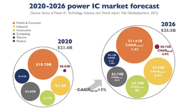
In their published analysis report, analysts at Yole stated that the total power IC market is expected to exceed $25.5 billion by 2026, with a CAGR of 3% between 2020 and 2026. Of course, not all power IC markets will grow at the same rate. The automotive industry will see the largest growth of all industries. The mobile and consumer market, though growing below average, is the largest at more than $10 billion, accounting for more than 40% of the total power IC market.

The power IC market will grow by 3% from 2020 to 2026, with mobile and consumer applications taking the largest share
The topic returns to power management for wearables. As we all know, power management must be considered an advanced strategy at the beginning of the development of wearable medical devices. While most modern microcontrollers are designed with low-power applications in mind, it is still critical to develop efficient power management solutions to minimize power consumption and extend battery life. Many would argue that battery life is also a key issue in wearables, and that thoughtful battery planning is critical to the success of wearables, especially wearable medical devices. Taken together, choosing the right battery and implementing proper power management are the major challenges of designing wearable devices.
Small wearable devices such as smartwatches or exercise belts, for example, typically can only accommodate single-cell lithium-ion batteries with a voltage of 3.8V and a capacity of 130mAh to 410mAh. Their battery management and charging systems must closely monitor changes in current, voltage and temperature at all times while the device is running and being charged. The ideal power management solution ensures that the system consumes as little power as possible and that charging is done as quickly and safely as possible.
The Texas Instruments (TI) TPS65070 is a chip with a battery charger, three step-down converters, and two Ldos designed specifically for single-chip power management in portable applications. The device can be powered while charging either by the USB port on the pin or by the DC voltage from the wall adapter connected to the pin AC. Three efficient 2.25MHz step-down converters are designed to power the processor, memory, and I/O. The step-down converter enters low-power mode under light load to achieve maximum efficiency over the widest possible range of load currents.
STMP30 developed by STMicroelectronics is also a power management chip that can effectively improve the battery running time of portable devices. The product has an input voltage range of 2.9V to 4.8V and includes three integrated DC/DC converters to provide all the power rails needed for AMOLED displays in smartphones and other portable devices.
Unlike other devices that anchor the VOUT1 at 4.6V, the 550mA VOUT1 boost converter provides adjustable output voltages that can be set between 4.6V and 5.0V in increments of 100mV, effectively optimizing display brightness for the lowest power consumption and best visibility in all conditions. The remaining two 550mA output single-phase step-boost inverter converters are provided with a programmable range of -0.8V to -6.6V, and 5.5V to 7.9V and 150mA, with the output voltage programmed via an external pin using a single wire (S-Wire) protocol
SIMO PMIC: Small and efficient power supply design solution
Lightweight and compact wearable devices typically use tiny batteries. Although battery capacity has increased over the past decade, the amount of stored power is quickly depleted in the limited time available. Designers of permanent wearables and Internet of Things (IoT) devices aim to extend battery life while reducing physical size. Small size and highly integrated power management IC (PMIC) is the preferred solution to achieve this goal.
PMIC is a highly integrated power supply product. It encapsulates the traditional multi-output power supply in a single chip, so as to achieve high efficiency in multiple power application scenarios, especially those powered by batteries, with a small volume. It not only optimizes the internal layout of the equipment, but also maximizes the energy efficiency and effectively prolongs the life of the battery.
DC-DC converter is the most commonly used PMIC in electronic products and has become a major force in the market in recent years due to its high conversion efficiency. DC-DC converters can be divided into linear voltage regulator (LDO), inductive buck/boost switch DC-DC regulator and capacitor switch DC-DC regulator according to the different operating modes and energy storage components. The three different architectures of DC-DC converters are different in terms of physical size, flexibility, and efficiency. Among them, LDO can be fully integrated and has good voltage scalability, but not high efficiency; Capacitive switching regulators (also known as charge pumps) can be fully integrated, high efficiency, but voltage scalability is poor; Inductive switching regulators are highly efficient and adjustable, but have the disadvantage that they are not fully integrated. Therefore, most wearables at this stage choose linear LDO and inductive switch voltage regulators (Buck/Boost), both of which can provide the flexible power management required by the design.
In the design of wearable devices, there is a trade-off between choosing a linear LDO or an inductive step-up/boost topology. In traditional inductive switching regulator structures, each output requires a separate inductor, and these inductors are often bulky and expensive, making them very difficult to miniaturize the device. In order to reduce the size, people often choose the compact, low noise LDO, but the loss of LDO is relatively high. The question is, how should designers balance the two? Is there a solution that is the best of both worlds?
The answer: Single-inductance multi-output (SIMO) regulators can solve this problem by addressing both size and energy efficiency.
Pmis based on SIMO architecture use a single inductor as an energy storage element to support multiple independent DC outputs. Compared to traditional inductive DC-DC switching regulators, SIMO architecture PMIC provides multiple outputs through a single inductor, integrating functions that would otherwise require multiple discrete components into a smaller package, saving space while still maintaining high efficiency
From ADI MAX77659
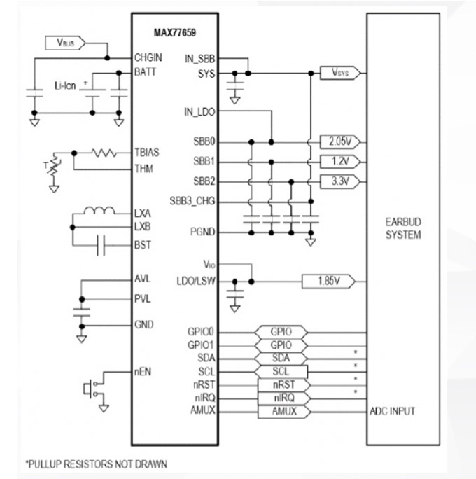
ADI's MAX77659 is a Single Inductor Multiple Output (SIMO) PMIC with an integrated switch mode step-boost charger that provides over four hours of power supply in just 10 minutes of charging and uses a single inductor to power multiple power rails, reducing the bill of Materials (BoM) by 60% and reducing total solution size by 50%. Compared to other current Pmics, it can be used very conveniently for wearables and Internet of Things devices in a smaller space. The MAX77659 integrates a switch mode step-down booster charger and three independently programmable step-down booster regulators, sharing a single inductor. The regulator operates at 91% efficiency under medium to heavy load conditions and consumes only 5.0μA of static current under light load conditions, extending battery life.
With SIMO PMIC, ADI has a broad portfolio of products such as MAX77640/MAX77641 and MAX77680/MAX77681, which reduce the size of power management circuits by nearly half and widely support space-constrained applications such as wearables, smart homes, etc.

MAX77659 working block diagram
From Texas Instruments TPS65135
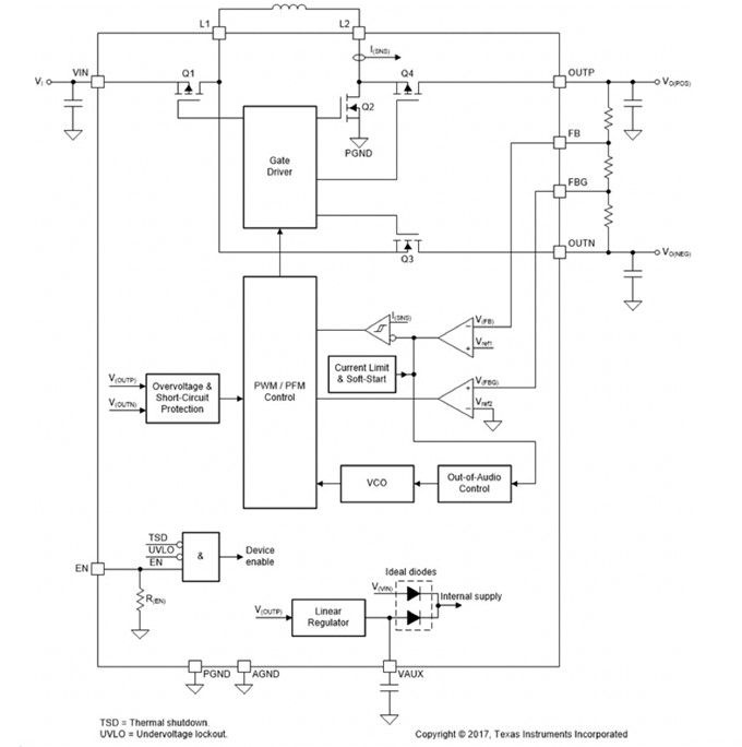
The TI Dual Power converter TPS65135 features a single inductor and multiple output (SIMO) topology with minimal use of external components, and generates a positive and negative output voltage above or below the input power supply voltage through a step-down/step-up topology. Derived from the SIMO topology, the TPS65135 has excellent line transient regulation. The product can be used to generate shunt rail power from 2.5V to 5.5V input supply voltages and is optimized for 3.3V rails for single-cell lithium-ion batteries.
The TPS65135 operates in a step-boost topology, using only 2.2µH inductors to generate positive and negative output voltages. It can produce positive output voltages of up to 6V and negative voltages as low as -7V (i.e. the input supply voltage may be higher or lower than the positive output voltage) through step-ups when the output loss is 50% or lower. Both outputs are controlled by EN pins, i.e. both outputs are enabled at high logic level and disabled at low logic level. The integrated UVLO feature disables the device when the input voltage is too low to function properly.

System block diagram of TPS65135
As a result, global spending on wearable technology is expected to reach $90 billion by 2022, and increase over time, according to Statista. Thin, small, and light are the physical requirements of wearables and the main reason why today's wearable technology limits battery life. Traditional batteries, such as lithium-ion coin batteries, may work well for sensors and other low-power wearables, but they struggle to meet the demands of more powerful wearables such as fitness bands and smartwatches.
Extending battery life is crucial for such devices to gain market acceptance, and no one wants a smart wearable's battery to run out in a matter of hours. However, the complex internal structure of the battery will greatly increase the size and cost of the device, making it inconvenient for people to wear it. To enable wearables to run for a long time, energy capture, battery management, power management and low power consumption solutions are all effective measures to extend the battery life of wearables.
It is clear that when developing wearables, battery selection and power consumption management are key to the overall success of the device. The challenge for the engineering and design teams is to carefully balance the variables in each device to meet all requirements and provide a limited amount of power depending on the battery selected. The SIMO PMIC solution not only improves the energy efficiency of the device, but also greatly reduces the size of the circuit board due to its high degree of integration. It is the ideal solution for power management of battery powered devices.
| Référence | Description | |
|---|---|---|
| TPS74601PBDRVT Texas Instruments |
PMIC - Régulateurs de tension - Linéaires, PWR MGMT SWITCHING REGULATOR | RFQ |
| TPS7B8233QDGNRQ1 Texas Instruments |
PMIC - Régulateurs de tension - Linéaires, PWR MGMT SWITCHING REGULATOR | RFQ |
| TPS74501PDRVT Texas Instruments |
PMIC - Régulateurs de tension - Linéaires, PWR MGMT SWITCHING REGULATOR | RFQ |
| TPS7B8250QDRVRQ1 Texas Instruments |
PMIC - Régulateurs de tension - Linéaires, PWR MGMT PWR DISTRIBUTION | RFQ |
| TPS7B8233QDRVRQ1 Texas Instruments |
PMIC - Régulateurs de tension - Linéaires, PWR MGMT PWR DISTRIBUTION | RFQ |
| MAXQ61HX-2620+ Maxim Integrated |
Embarqués - Microcontrôleurs, MODULE MCU 16BIT | RFQ |
| MAXQ61HX-2597+ Maxim Integrated |
Embarqués - Microcontrôleurs, MODULE MCU 16BIT | RFQ |
| MAXQ61HX-2594+ Maxim Integrated |
Embarqués - Microcontrôleurs, MODULE MCU 16BIT | RFQ |
| MAXQ61HX-2047+ Maxim Integrated |
Embarqués - Microcontrôleurs, MODULE MCU 16BIT | RFQ |
| MAX3845UCQ+ Maxim Integrated |
Linéaire - traitement vidéo, DVI/HDMI 2:4 TMDS FANOUT SWITCH | RFQ |
Traction inverters are the main battery drain components in electric vehicles (EVs), with power levels up to 150kW or higher. The efficiency and performance of traction inverter directly affect the driving range of electric vehicle after a single charge. Therefore, in order to build the next generation of traction inverter systems, silicon carbide (SiC) field effect transistor (FET) is widely used in the industry to achieve higher reliability, efficiency and power density.
Do you know the 8 application circuits of operational amplifiers?
This technical presentation requires an understanding of how to configure an operational amplifier in a typical gain control circuit. The applications of linear and nonlinear digital potentiometers are discussed. This article gives an overview of the basic techniques required to convert audio and other potentiometer/op amp applications from conventional mechanical potentiometers to solid state potentiometers
The current in an electronic circuit usually has to be limited. In USB ports, for example, excessive current must be prevented to provide reliable protection for the circuit. Also in the power bank, the battery must be prevented from discharging. Too high discharge current results in too large voltage drop of the battery and insufficient supply voltage of downstream devices
Using advanced real-time control technologies such as motor control circuits with higher power density, higher integration and more efficient systems, better acoustic performance of the system can be achieved
Brushless direct current (BLDC) motors have been widely used in household appliances, industrial equipment and automobiles. While brushless DC motors offer a more reliable and maintainable alternative to traditional brushless motors, they require more sophisticated electronics to drive them
How to achieve precise motion control in industrial actuators
The NCP51820 is a 650 V, high-speed, half-bridge driver capable of driving gallium nitride (" GaN ") power switches at dV/dt rates up to 200 V/ns. The full performance advantages of high voltage, high frequency and fast dV/dt edge rate switches can only be realized if the printed circuit board (PCB) can be properly designed to support this power switch. This paper will briefly introduce NCP51820 and the key points of PCB design of high performance GaN half bridge grid driver circuit using NCP51820