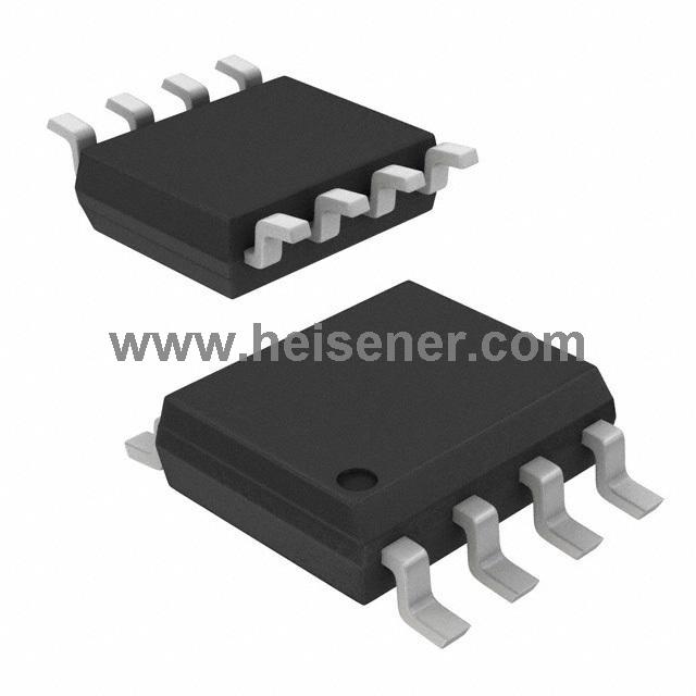
IR2184S Introduction
The IR2184S is a high-speed, high-voltage power MOSFET and IGBT driver, designed for driving both high-side and low-side channels in power electronics applications. It utilizes proprietary HVIC and latch-immune CMOS technologies, providing a rugged, monolithic construction that ensures reliable performance even in challenging environments. The driver is compatible with standard CMOS or LSTTL logic inputs, supporting voltages as low as 3.3V.
With a high pulse current buffer stage, it minimizes cross-conduction between the low and high sides, improving efficiency and reducing heat generation. The IR2184S can drive N-channel MOSFETs or IGBTs in high-side configurations, supporting voltages up to 600V. This makes it ideal for use in applications like motor control, inverters, and industrial power supplies, where efficient and reliable switching is essential for optimal system performance.
IR2184S Pinout

1. IN – Input for the logic signal to drive the high and low-side MOSFETs.
2. SD – Shutdown pin. When pulled low, it disables the outputs (LO and HO) and the internal logic.
3. COM – Common pin for the low-side driver. Connects to the low-side ground.
4. LO – Low-side output pin for driving the low-side MOSFET.
5. VCC – Power supply for the low-side driver circuitry (typically 10-20V).
6. VS – Source of the high-side MOSFET. Connects to the switching node of the high-side MOSFET.
7. HO – High-side output pin for driving the high-side MOSFET.
8. VB – Floating bootstrap pin for providing the gate drive to the high-side MOSFET.
IR2184S Marking Information

IR2184S Typical Application

IR2184S Functional Block Diagram

IR2184S Specification
| Specification | Value |
| Number of Drivers | 2 |
| Supply Voltage | 10V ~ 20V |
| Logic Voltage - VIL, VIH | 0.8V, 2.7V |
| High-Side Driver Voltage | 600V (maximum) |
| Low-Side Driver Voltage | 10V |
| Peak Output Current | 1.9A (Source), 2.3A (Sink) |
| Rise / Fall Time (Typ) | 40ns, 20ns |
| UVLO (Under Voltage Lockout) | VCC = 8V (typical) |
| Operating Temperature Range | -40°C ~ 150°C |
| Input Voltage Threshold (Logic) | 2.0V (minimum) |
| Package Type | 8-SOIC |
IR2184S Features
Floating channel designed for bootstrap operation
Fully operational to +600V
Tolerant to negative transient voltage dV/dt immune
Gate drive supply ranges from 10 to 20V
Undervoltage lockout for both channels
3.3V and 5V input logic compatible
Matched propagation delay for both channels
Logic and power ground +/- 5V offset.
Lower di/dt gate driver for better noise immunity
Output source/sink current capability 1.4A/1.8A
Also available LEAD-FREE (PbF)
IR2184S Applications
Motor Drives
Power Inverters
Class D Audio Amplifiers
Switching Power Supplies
Induction Heating
H-Bridge Circuits
Switch Mode Power Supplies (SMPS)
Industrial Automation and Robotics
Power Factor Correction (PFC)
High-Speed Switching Circuits
IR2184S Package
The IR2184S comes in an 8-SOIC package, which is compact and highly reliable, making it ideal for space-constrained applications. The package dimensions are 4.90mm × 6.00mm × 1.75mm, suitable for automated placement and high-density PCB designs. The 8-SOIC package features 8 pins, with a standard pin spacing of 1.27mm. Its maximum operating temperature range is typically from -40°C to +125°C, making it suitable for a variety of industrial and consumer electronic environments.

How to Use IR2184S?
When using the IR2184S, the first step is to correctly connect the circuit and power supply. Begin by connecting the power supply voltage (VCC) and ground (COM) pins to an appropriate power source. Next, connect the control signal (IN) to a suitable logic input, which can be a standard CMOS signal at 3.3V or 5V. This input is used to control the switching of the high-side and low-side MOSFETs or IGBTs.
Then, connect the high-side driver signal (HO) and low-side driver signal (LO) to the gate of the MOSFETs or IGBTs. Ensure that these driver signals operate within the required voltage range. By properly configuring these pins, the IR2184S can drive both high-side and low-side power semiconductors, allowing for effective current control and switching, thereby ensuring the safety and efficient operation of the system.
IR2181/IR2183/IR2184 Comparison

FAQs
What can IR2184S do?
The IR2184S is a high voltage, high-speed MOSFET and IGBT driver used for controlling high and low-side power MOSFETs or IGBTs in various applications like motor drives, inverters, and other power electronics. It allows for efficient switching of power devices, especially in configurations where both high-side and low-side switching is required.
What types of devices can be controlled by the IR2184S?
The IR2184S is capable of driving N-channel MOSFETs and IGBTs in both high-side and low-side configurations, providing flexible control for power semiconductors in various applications.
How do I connect the IR2184S to power MOSFETs or IGBTs?
To use the IR2184S, you will need to connect the VCC and COM pins to your power supply, and the logic input (IN) to the control signal. The HO (high-side output) and LO (low-side output) pins should be connected to the gate of the respective MOSFETs or IGBTs.