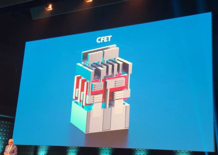
The chip industry’s big three—Intel, Samsung and Taiwan Semiconductor Manufacturing Co. (TSMC)—are “getting serious” about a new 3D device architecture that promises to solve scaling problems that persist with today’s state-of-the-art nanosheet technology, experts told EE Times.
The three largest chipmakers for the first time gave presentations in one session at the International Electron Devices Meeting (IEDM) last month, suggesting they will commercialize complementary field effect transistor (CFET) architecture within a decade, according to Naoto Horiguchi, director of the CMOS device program at global R&D organization imec.
“All the big players–Intel, Samsung, TSMC–showed their latest achievement results,” Horiguchi said. “This is the first time the ‘big three’ presented results in one session. They are getting more and more serious.”
Before the CFET era arrives, the industry will endure three generations of nanosheet architecture and related problems with CMOS components like SRAM that have stopped scaling down. That halt in scaling will force designers of high-performance computing chips to disaggregate CMOS functions like SRAM, with workarounds that splice together older technology nodes and chiplets, according to imec, which developed the CFET concept around 2016.
“Some legacy technology like analog or I/O may have to be integrated by different schemes,” Horiguchi added. “An example is to integrate analog or I/O by using chiplet technology. At least some of the logic and SRAM can be scalable by using CFET architecture. That’s our current expectation.”
Slowing process shrinks
Until 2032, imec expects, the speed of process-node shrinks will slow, forcing greater reliance on the mix-and-match use of chiplets and advanced packaging combined with those high-performance logic components that do continue scaling down.
“CMOS device scaling with nanosheet only is very difficult,” Horiguchi said. “With CFET, we can seriously continue device scaling and then, of course, combine this with some other technology like chiplets and advanced packaging to improve chip performance. CFET is creating a path for continuous device scaling. That’s the selling point of CFET.”
Imec expects CFET to take device architecture beyond the 1-nm node by around 2032. Samsung was the first to introduce nanosheet/gate all around architecture at the 3-nm node in 2022. TSMC will introduce nanosheet with its 2-nm node in 2025, TSMC said.
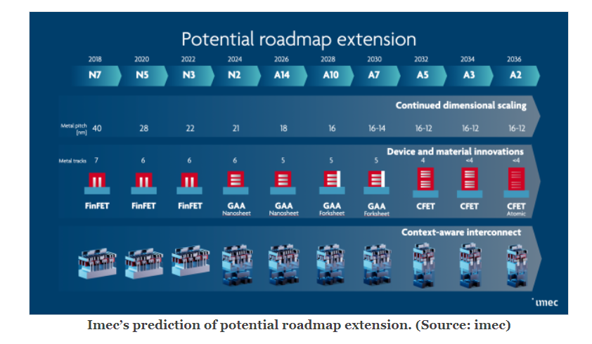
Horiguchi noted contacted poly pitch (CPP)—the distance from one transistor gate to the next—as a key metric for CMOS device scaling.
“The key players showed CPP of 48-45 nm. It’s close to the target dimensions for CFET products,” he said. “To make this big shift into smaller dimensions, [Intel, Samsung and TSMC] must have several process innovations, process improvements and so forth. They will not talk about these process innovations, but without this progress, they probably cannot make such devices.”
The three chipmakers have probably moved their CFET development from the laboratory to pilot lines close to industry standard, Horiguchi said.
Last month, Intel told EE Times it’s made a unique breakthrough in 3D stacked NMOS (N-channel metal-oxide semiconductor) on PMOS (P-channel metal-oxide-semiconductor) transistors combined with backside power and backside contact to maximize area and power delivery efficiencies.
In the CFET architecture, NMOS and PMOS devices are stacked atop each other.
In a summary of TSMC’s work, Szuya Liao, a TSMC director of device architecture pioneering, said in prepared remarks that the company has reached the 48-nm CPP mark that Horiguchi described as a key threshold.
“By introducing critical vertical isolations between NMOS/PMOS FETs and proper inner spacer between gate and source/drain, our vertically stacked nFET-on-pFET nanosheet transistors yield a survival rate of over 90% and demonstrate high on-state current with low leakage, achieving a healthy six-order of magnitude on/off current ratio,” she said.
By stacking n-type and p-type FETs vertically, the footprint can be cut in half and transistor count doubled, Liao said.
“This is like increasing urban density by building two townhouses on the same footprint as one single-story unit,” Liao said.
Samsung didn’t respond to a request for comment.
More hurdles to clear
While CFET promises to resume the pace toward process shrinks, several hurdles remain before the new architecture is commercialized, according to Dylan Patel, chief analyst at SemiAnalysis.
“There’s a whole host of other challenges with CFET that make it much more difficult to manufacture,” he told EE Times. “How you get power to the CFET structure is very difficult and complicated. There are different integration schemes of backside power delivery. It’s very difficult for large, complex companies to jump to CFET.”
Frontside processing and backside processing aren’t completely equal, Horiguchi said.
“With the frontside process, we can squeeze all the metal lines in a very accurate overlay, but backside, we may have some misalignment issues,” he said. “Some wafer distortion in frontside processing could happen, which causes larger misalignment in backside processing. That’s exactly what we are studying today.”
Taller townhouses
CFET structures are taller than the 3D shapes in nanosheet architecture, Horiguchi said. The increased aspect ratio of the structures creates fabrication challenges.
“Patterning is the first challenging part,” he added. “That’s making all the aspect ratios double. Patterning has to be somehow improved or innovated to enable this shift.”
High aspect ratios will require deposition of dielectric, metal and some epitaxial growth to have a source gain at the very bottom of a trench, Horiguchi noted.
Innovations in materials and process are other manufacturing hurdles, he said.
“We need very high dopant activations and then also very low contact resistivity,” Horiguchi said. “We need to provide special high-k/metal gate for CFET. These also have to be enabled in very tall structures. That’s probably the key challenge: in a very tall and stacked device architecture.”
Imec is working with materials and equipment suppliers like Applied Materials, Tokyo Electron and Lam Research to develop CFET manufacturing tools.
The “significant challenges” of the CFET architecture may lead to increased process complexity and cost, TSMC said.
“To overcome these challenges, it is essential to choose carefully the integration schemes that reduce process complexity and minimize the demand for new materials and process capabilities,” Liao said. “It is also important to engage in early EDA/flow tool development to prepare for major design changes.”
About US
Heisener Electronic is a famous international One Stop Purchasing Service Provider of Electronic Components. Based on the concept of Customer-orientation and Innovation, a good process control system, professional management team, advanced inventory management technology, we can provide one-stop electronic component supporting services that Heisener is the preferred partner for all the enterprises and research institutions.