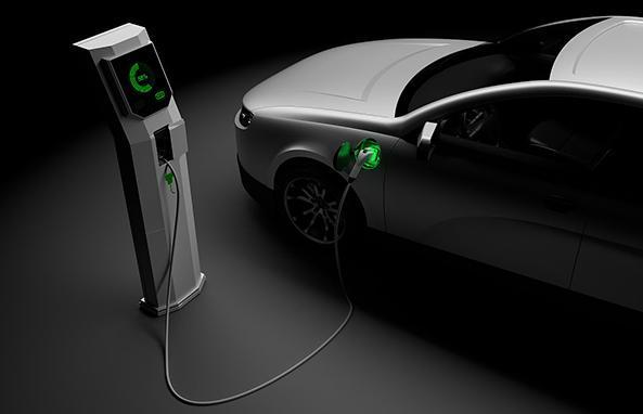
To reduce the time required to charge, the industry is using DC fast chargers (DCFCs) and ultra-fast chargers. The DCFCs and ultra-fast chargers bypass the on-board chargers of electric vehicles and provide more power directly to the battery, which can be charged at a rated current of 200-500 A, depending on the capacity of the battery.
Overview of DCFCs
To enhance charging speed, support increased EV battery voltages and enhance overall power efficiency, DCFCs must operate at high voltages and power levels. This poses a problem for original equipment manufacturers, as they must provide a framework that maximizes efficiency while ensuring both reliability and safety are not compromised.
DCFCs and ultra-fast chargers incorporate several components (Figure 1), including auxiliary power, sensing, power management, networking and communications. The complexity of their design is related to the requirement of addressing the charging requirements of different EVs.

Most of the new DCFCs are designed with dual combined charging system connectors equipped with 24 feet of cable. These chargers can charge an electric vehicle at a rate of 100a to 300a, depending on the capacity of the electric vehicle battery. The next generation DC ultra-high speed chargers can be charged at large currents of up to 500 A and provide 400 kW of output power.
Design considerations
Designing a DC fast charger requires the consideration of key factors including:
● Efficiency: To maximize power delivery, it is important to design the charging system for the power level at which efficiency has the most significant effect.
● Discrete or integrated solutions: Discrete designs provide optimal adaptability but necessitate a more intricate development procedure. Modules provide numerous performance advantages that are challenging to get with a discrete design, including a streamlined mechanical assembly, enhanced thermal management, increased dependability and diminished voltage spikes, and high-frequency electromagnetic interference.
● Topology: The topology, whether it is two-level or three-level, and the requirement for unidirectional or bidirectional operation will have a direct impact on the selection of components for the charger.
Numerous topologies exist for the implementation of the power-factor correction (PFC) and DC/DC stages of a DC charger. This article, based on an onsemi white paper, will provide a comprehensive analysis of different standalone DC/DC topologies employed in this specific application.
Main types of topologies
Galvanic isolation is necessary between the mains grid and the battery to prevent the grounding of EV batteries. Isolation is a compulsory requirement in the DC/DC power stage of an EV DCFC.
Full-bridge LLC
The topology comprises a primary full-bridge circuit, resonant LLC tanks and a secondary full-bridge rectifier, as depicted. The LLC converter facilitates zero-voltage switching (ZVS) on the primary side and zero-current switching (ZCS) on the secondary side. Variable-frequency operation is required to control the output voltage. The LLC topology is suggested for applications with a small output voltage range and a set input voltage to achieve great efficiency.
Interleaved three-phase LLC resonant converter
This converter provides optimal efficiency under full-load conditions by evenly dispersing losses among three phases. Additionally, it mitigates stress on the capacitor and power switches. Nevertheless, this configuration exhibits diminished efficiency due to a decrease in charging current as the battery reaches its rated voltage.
To enhance overall efficiency under various load conditions, it is necessary to apply phase shedding. The operation of both dual-phase and single-phase resonant converters will result in excellent efficiency at both 50% load and low-load conditions. Additionally, these converters will ensure output voltage regulation even at low loads.
PSFB converter
The phase-shifted full-bridge (PSFB) converter comprises a main full-bridge circuit, a resonant inductor, a secondary rectification bridge and an LC filter. The system provides ZVS performance for the major switches by utilizing phase-shift control and eliminating turn-on losses.
Nevertheless, this configuration will result in substantial power dissipation during the switching-off process for the primary switches and the output rectifier. To mitigate voltage overshoot in output diodes, it is necessary to use either active or passive snubbers. PSFB converters are highly efficient for charging high-voltage batteries.
DAB converter
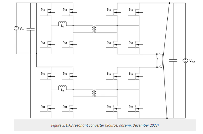
Figure 2 shows the components of the dual active bridge (DAB) converter, including a primary full bridge, a leakage inductance from the transformer, a secondary full bridge and a filter capacitor. The system does not require any extra resonant components. Instead, it utilizes the transformer’s leakage inductance and the output capacitance of the power switches to accomplish soft-switching operation. The advent of wide-bandgap semiconductors has contributed to the increasing popularity of DAB converters in applications involving bidirectional power flow.

The DAB converter accomplishes ZVS for the primary switches and ZCS for the secondary bridge switches. This converter exhibits reduced switching losses but experiences elevated conduction losses.
Utilizing low-RDS(on) silicon carbide MOSFETs in the secondary bridge circuit, such as onsemi’s EliteSiC, a decrease in conduction losses is enabled. The DAB converters offer superior compactness, efficiency, reduced component strain and smaller filter elements compared with alternative topologies.
Interleaved DAB converter
Interleaved DAB converters can be employed to attain power levels exceeding 75 kW. This topology divides losses between two transformers and enables the utilization of cost-optimized onsemi’s EliteSiC full-bridge power integrated modules. The EliteSiC F2 full-bridge power integrated modules can reach a power output of 60 kW. To provide a 360-kW DC fast-charger system, it is possible to connect and operate six charger system modules, each with a capacity of 60 kW, in parallel.
DAB resonant converter
The DAB resonant converter is an alternative method to the DAB converter for achieving bidirectional power flow. To achieve the DAB resonant converter, a supplementary resonant network (LC, LLC and CLLC) is incorporated into the DAB converter.
The CLLC DAB converter (Figure 3) exhibits symmetrical circuitry, resulting in identical voltage gain characteristics for power flow in both directions. CLLC converters employ a pair of resonant capacitors positioned on either side of the transformer, hence mitigating the strain on the capacitors compared with an LLC converter.
EliteSiC power integrated modules (half-bridge or full-bridge) are recommended for high-power DAB CLLC resonant converter applications, delivering 25 kW to 120 kW (using three-phase interleaved dual active half-bridge resonant converter) output power.
Three-level DNPC LLC resonant converter
This converter comprises a three-level half-bridge circuit, clamped diodes, a resonant LLC network and a secondary full-bridge circuit. It is chosen as the principal topology for the primary side of the resonant LLC circuit due to its identical construction to the phase leg of the rectified PFC front end and two-level complete bridge.
SHB LLC resonant converter
This is an alternative kind of multi-level topology that can be employed as a primary-side topology for LLC circuits to endure high input voltage. The series half-bridge (SHB) LLC shares the identical resonant tank and secondary full-bridge circuit with the DNPC resonant LLC design.
The primary benefit of the SHB LLC phase leg is the elimination of two clamping diodes compared with the DNPC LLC phase leg, resulting in a reduction in the overall number of components. SBH circuits have a simpler construction compared with the DNPC topology, which is its main advantage.
Conclusion
According to onsemi, the DAB converter topology provides an optimal solution with the capacity to transfer power bidirectionally. The DAB converter reduces the number of components and eliminates series resonant capacitors in high-power DCFC applications.
Onsemi has developed the 25kW DC Fast Charger reference design utilizing the NXH010P120M3F1 half-bridge SiC module to showcase this configuration. An interleaved DAB converter is an appropriate topology for devices above 100 kW.
About US
Heisener Electronic is a famous international One Stop Purchasing Service Provider of Electronic Components. Based on the concept of Customer-orientation and Innovation, a good process control system, professional management team, advanced inventory management technology, we can provide one-stop electronic component supporting services that Heisener is the preferred partner for all the enterprises and research institutions.